Tin sulfide (SnS) is an abundant, safe, and environmentally friendly solar cell material. This inexpensive material is forecast to be used in next-generation solar cell panels.
A research group led by Issei Suzuki and Sakiko Kawanishi, assistant professors at Tohoku University’s Institute of Multidisciplinary Research for Advanced Materials, has fabricated n-type conductive SnS thin films by impurity doping for the first time.
Conventional SnS thin films are usually p-type conductive. Thus, SnS thin-film solar cells have been fabricated using a pn heterojunction with p-type SnS thin film and other n-type semiconductor thin films, such as CdS. However, the conversion efficiency of such heterojunction devices has stagnated at approximately 5%, rendering their use impractical.
The SnS thin-film solar cells employing a pn homojunction, which uses SnS thin films for both p-type and n-type layers, is expected to exhibit higher conversion efficiency. Yet, n-type conducive SnS thin films without toxic elements have never been achieved before.

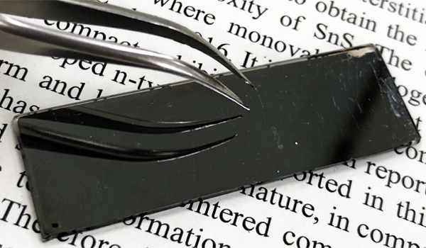
The world’s first n-type conductive SnS thin film without containing toxic elements. ©Issei Suzuki et al.
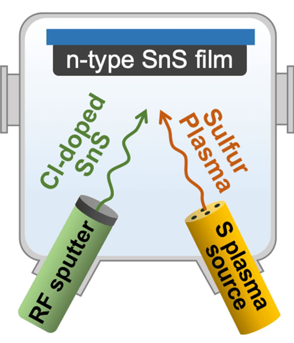
Utilizing chlorine-doping and a sulfur plasma supply, the research group reduced the lattice defects inhibiting the n-type conversion of SnS, realizing the world’s first n-type SnS thin films without toxic elements.

A schematic illustration of the new technique used to fabricate n-type SnS thin films. The n-type conductive SnS thin films were achieved by fabricating thin films of chlorine(Cl)-doped SnS with a supply of sulfur plasma. ©Issei Suzuki et al.
“Our realization paves the way for practical pn homojunction SnS thin-film solar cells,” said Suzuki.
The results of the research were published in Physical Review Materials on December 9, 2021.
Publication Details:
“N-Type Electrical Conduction in SnS Thin Films”
Issei Suzuki, Sakiko Kawanishi, Sage R. Bauers, Andriy Zakutayev, Zexin Lin, Satoshi Tsukuda, Hiroyuki Shibata, Minseok Kim, Hiroshi Yanagi and Takahisa Omata
Physical Review Materials
DOI: 10.1103/PhysRevMaterials.5.125405
▶ Tohoku University
▶ Atomic Site Control in Inorganic Materials (OMATA LABORATORY)
▶ Materials Separation Processing (SHIBATA LABORATORY)
Contact
Institute of Multidisciplinary Research for Advanced Materials (IMRAM), Tohoku University
Email: issei.suzuki[at]tohoku.ac.jp
Website: https://www2.tagen.tohoku.ac.jp/lab/omata/english/
Sakiko Kawanishi
Institute of Multidisciplinary Research for Advanced Materials (IMRAM), Tohoku University
Email: s-kawa[at]tohoku.ac.jp
Website: https://www2.tagen.tohoku.ac.jp/lab/shibata/english/