Research
研究概要:透過電子顕微鏡・ナノ電子プローブを用いた局所構造・静電ポテンシャル分布解析
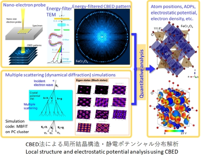 機能性材料において、ナノスケールの局所構造や結晶・ドメイン界面に起因する特異な物性の報告が増加しており、局所結晶構造解析の重要性が高まっています。このためには、透過電子顕微鏡を利用して、ナノサイズに収束した電子プローブを試料に照射する収束電子回折(CBED)法がきわめて有利です。本研究分野では、CBED法を用いて動力学回折(多重散乱)理論計算に基づく定量的な局所結晶構造解析を世界に先駆けて実現し、強誘電セラミックス材料、固体燃料電池関連材料、強相関電子系材料等に適用しています。現在、走査透過電子顕微鏡(STEM)法とCBED法を組み合わせたSTEM-CBED/4D-STEM法を活用して、結晶界面・ナノドメイン構造のような非周期・不均一構造から局所結晶構造・静電ポテンシャルの空間変化を定量解析する手法の開発に取り組んでおり、局所構造・界面に起因する新規機能性材料開発に寄与することを目指しています。
主な研究テーマ
- 収束電子回折法による局所結晶構造・静電ポテンシャル分布解析法の開発と応用: Development of local crystal structure and electrostatic potential analysis and its applications
- 4D-STEM法による結晶界面・ナノドメイン構造の局所構造・静電ポテンシャル分布解析: Local structure and electrostatic potential analysis of crystal interface and nanodomain structures using 4D-STEM
- 深層学習との共創による局所構造解析手法の開発: Development of a Local Structure Analysis Method Assisted by Deep Learning
- 機能性材料の外場印加におけるナノ局所結晶構造解析: Nanoscale local crystal structure analysis of functional materials under applying external fields
- 構造相転移におけるナノ局所結晶構造解析: Nanoscale local crystal structure analysis at structural phase transformations
現在進行中の主なプロジェクト
- 深層学習駆動型QCBED法による多パラメータ局所構造解析 2026.4-2028.3 JSTさきがけ融合研究加速支援 研究代表者 森川大輔
- 超原子座標構造の可視化による創薬の革新 2023.4-2028.3 JST未来社会創造事業 研究代表者 米倉功治、研究分担者 津田健治「精密構造解析」
- 革新的電子密度マッピング技術の構築:4D-STEMによる界面・欠陥の定量自動解析 2025.10-2027.9 NEDO若サポ マッチングサポートフェーズ 研究代表者 森川大輔
終了した主なプロジェクト
- 二次元配列構造における局所電子密度分布および物性解析手法の開発 2022.10-2026.3 JSTさきがけ 研究代表者 森川大輔
- ナノ電子プローブによるマルテンサイト相転移の局所構造解析と微視的相転移機構 2022.4-2024.3 基盤研究(B) 研究代表者 津田健治
- 高クロム鋳鉄カーバイド添加元素のマルチ電子プローブ局所結晶構造解析 2023.4-2024.3 挑戦的研究(萌芽) 研究代表者 津田健治
- 局所電子密度分布解析による強誘電体ドメイン壁における分極回転の直接観測 2022.4-2023.3 新学術領域研究(公募) 研究代表者 森川大輔
共同研究の例:
東北大学 寺内研究室、米倉研究室、福山研究室、佐藤(卓)研究室、松岡研究室
名古屋大学 武藤研究室、斎藤研究室
東京大学 溝口研究室、幾原・柴田研究室
静岡大学 符研究室
日本大学 橋本研究室
オーストラリア モナシュ大学 A.Prof. Philip Nakashima
ドイツ フンボルト大学ベルリン Prof. Christoph Koch
アメリカ ブルックヘブン国立研究所 Dr. Yimei Zhu
日本電子 次世代電子顕微鏡技術共同研究部門
他にも国内国外の大学や企業との共同研究を進めています。
研究キーワード
電子線結晶学、収束電子回折、STEM-CBED/4D-STEM、構造相転移、結晶界面・ドメイン構造
所属学会
Nanoscale local crystal structure and electrostatic potential analysis using nano-electron probe
Local crystal structure analysis is increasingly important in functional materials that exhibit intriguing physical properties induced by nanoscale local structures and crystal interfaces. For this purpose, the convergent-beam electron diffraction (CBED) method using nano-electron probe is extremely advantageous. Using the CBED method, we developed a quantitative analysis method of local structures and electrostatic potential distributions based on the dynamical diffraction (multiple scattering) theory, and applied it to various functional materials. Furthermore, we are developing a method to investigate spatial variations of local structures and electrostatic potential distributions in crystal interfaces and nanodomain structures by using the STEM-CBED/4D-STEM method.
We welcome foreign students and postdoc researchers.
The following projects are ongoing.
+ Development of local electron density and physical property analysis method for two dimensional structure, Precursory Research for Embryonic Science and Technology, Japan Science and Technology Agency, 2022-2026, Daisuke MORIKAWA
+ Innovation of drug discovery through visualization of structures beyond atomic coordinates, Realization of common platform technologies, facilities and equipment
that create innovative knowledge and products, Japan Science and Technology Agency, 2023-2027, (Director) Koji YONEKURA, (Co-Investigator) Kenji TSUDA
Requirements:
(Student) Fundamental knowledge about solid state physics. Knowledge and experience with TEM are preferred.
(Postdoc) Fundamental knowledge about solid state physics, experience of using TEM or first-principle calculation or python scripting
Contact: D. Morikawa, daisuke.morikawa.e5@tohoku.ac.jp