Research
Research Topics
1. Surface Atomic Structure Analysis and Extreme Measurement of Electronic States Using STM
This research aims to develop ultra-high spatial resolution measurement techniques and atomic/molecular manipulation techniques that form the foundation of nanoscience, through the development of unique equipment centered on scanning tunneling microscopes (STMs). Specifically, we utilize scanning tunneling spectroscopy (STS) under cryogenic and ultra-high vacuum conditions to measure not only the geometric structure of single molecules but also their “electronic states,” such as local density of states and energy levels, with extreme precision. In particular, we will elucidate the effects of atomic defects and interface structures on carrier transport from a physical perspective, focusing on two-dimensional layered materials such as molybdenum disulfide (MoS2) and organic semiconductor molecules. Furthermore, based on the knowledge gained from these extreme measurements, we are developing next-generation devices that actively utilize the quantum mechanical properties of individual molecules. By constructing single molecules as functional units from the bottom up and controlling their internal degrees of freedom and spin states, we aim to create ultra-low power consumption, high-performance nanodevices that are difficult to achieve with conventional silicon technology. From exploring fundamental scientific principles to implementing innovative devices that maximize molecular characteristics, we consistently promote a new physical paradigm in the nanoscale.
2. Elucidating the correlation between atomic structure and carrier transport properties in two-dimensional layered materials such as molybdenum disulfide
Two-dimensional layered materials, exemplified by molybdenum disulfide (MoS2), possess both atomic-level thinness and excellent electrical and optical properties, attracting global attention as innovative semiconductor materials for the post-silicon generation. This research aims to elucidate the structural and property correlations of these two-dimensional materials, specifically how “fine disorder in the atomic arrangement” affects “macroscopic electrical conductivity” as a device. Specifically, we utilize scanning tunneling microscopy (STM) to visualize atomic defects, impurities, grain boundaries, and edge structures at the single-atom scale, precisely evaluating their impact on local electronic states (density of states). In parallel with the evaluation of these atomic and molecular structures and electronic states, we will measure the carrier mobility of field-effect transistors (FETs) and the temperature and electric field dependence of their conduction mechanism. By directly linking knowledge of microscopic atomic structure with macroscopic transport characteristics, we will identify mobility limiting factors and the physical origin of Schottky barriers. Through elucidating this correlation, we aim to establish defect control technologies and interface design guidelines to maximize the potential of two-dimensional materials, and to create foundational technologies for next-generation nanoelectronics that enable ultra-low power consumption and ultra-high-speed operation.
3. Photoresponsive, high-precision molecular sensing using atomic layer thin films
Currently, large spectroscopic devices are required for molecular identification, but if current detection can be easily performed with small sensors, it could bring about innovation in the medical, environmental, and agricultural fields. Molecules have a highest occupied orbital (HOMO) and a lowest unoccupied orbital (LUMO), and the energy difference between them (ΔE) is a physical quantity unique to the molecule. When a molecule absorbs light energy equal to ΔE, electrons and holes are generated, so by measuring the electrical signal while sweeping the light, the molecular species can be identified. In this study, we fabricated a field-effect transistor using a molybdenum disulfide (MoS2) thin film with several atomic layers. Conventional MoS2 sensors lack discriminatory ability because they rely solely on current changes associated with molecular adsorption. However, this study introduced a method to measure the “photoresponse current when irradiated with specific light.” Experimental results demonstrated, for the first time in the world, that a specific photoresponse current is generated when a thin film with adsorbed copper phthalocyanine molecules is irradiated with light of 1.76 eV, corresponding to its ΔE. This achievement enables electrically simple and highly accurate molecular identification. In the future, it is expected to have applications in next-generation sensing systems that address diverse social issues, such as early disease detection using wearable devices that constantly monitor bodily substances, detection of harmful gases, and monitoring of plant growth.
Figure A) When a molecule absorbs light equal to the energy difference between its highest occupied orbital (HOMO) and lowest unoccupied orbital (LUMO), a positively charged hole is generated in the HOMO, and a negatively charged electron is generated in the LUMO. B) When copper phthalocyanine molecules are adsorbed onto a MoS2 field-effect transistor and irradiated with 1.76 electron volt light, a photoresponse current is observed. C) Photoresponse current before and after adsorption of copper phthalocyanine molecules.
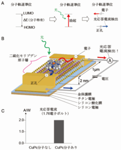
Figure A) When a molecule absorbs light equal to the energy difference between its highest occupied orbital (HOMO) and lowest unoccupied orbital (LUMO), a positively charged hole is generated in the HOMO, and a negatively charged electron is generated in the LUMO. B) When copper phthalocyanine molecules are adsorbed onto a MoS2 field-effect transistor and irradiated with 1.76 electron volt light, a photoresponse current is observed. C) Photoresponse current before and after adsorption of copper phthalocyanine molecules.
4. Nanoscale manipulation of surface chemical reactions based on the adsorption behavior and motion control of molecules
This research aims to achieve innovative surface chemical reaction control by understanding the series of processes of molecular adsorption, diffusion, and reaction on solid surfaces at the atomic level and actively manipulating them.
The foundation of this research is extreme measurement using a scanning tunneling microscope (STM). Not only is the adsorption orientation and electronic state of single molecules observed in real time, but nanoscale processes such as guiding molecules to targeted reaction sites and controlling atomic and molecular structures to be favorable for specific reactions are performed using atomic manipulation with probes. Furthermore, by utilizing supersonic molecular beam technology, which allows for precise control of the translational kinetic energy and internal state of gas molecules, we enable “energy-selective reaction control” by injecting molecules with specific kinetic energies onto a surface, thereby physically overcoming reaction barriers that could not be overcome by conventional thermal processes.
In addition, we plan to combine this with control by applying an external voltage to the solid surface, which is a major feature of this research. By dynamically controlling the Fermi level and charge density on the surface using field-effect transistor (FET) structures, we can freely modulate the strength of charge transfer and interactions with adsorbed molecules.
Through this tripartite approach of “local manipulation by STM,” “collision energy control by supersonic molecular beams,” and “electronic state modulation by external electric field,” we aim to completely control molecular motion and reaction pathways at the nanoscale. This research will not only provide design guidelines for highly efficient next-generation catalysts but also construct a new scientific principle for bottom-up functional material creation using atoms and molecules as building blocks.